SEMIPROBE MEMS-0515 Wafer Probe Station
 Introduction
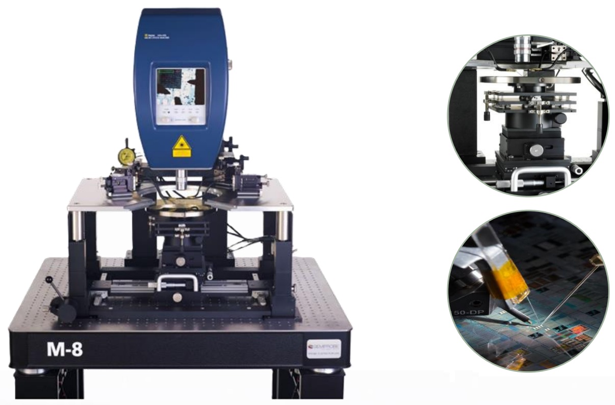
A precise manual wafer probe station called the SEMIPROBE MEMS-0515 was created for electrically characterizing semiconductor devices, MEMS, and nanomaterials. Its high-accuracy positioning probes controlled by micromanipulators make it perfect for failure analysis, process development, and research labs in cleanroom or laboratory settings.
Specification
Chuck Size: Maximum
Wafer Capacity: 150 mm (6″) XY
Stage Travel (manual control): 100 mm × 100 mm Z-Axis
Range: 25 mm (focus adjustment for the microscope)
Probe Holders: manual manipulators with four to eight positions ±1μm is the contact accuracy (with precise adjustability)
Platen Material: Ceramic or ground stainless steel (ESD-safe alternatives)
Operating Conditions: non-condensing, 15–30°C, <60% relative humidity
Features
- Precision Micromanipulators: sub-micron positioning tungsten or gold-tipped probes
- Anti-Vibration Design: Isolated base minimizes ambient noise
- ESD-Safe Options: shielded cables for delicate devices and grounded chuck
- Modular Design: Suitable for probe card adapters, vacuum chucks, and thermal chucks
- Support for Multiple Microscopes: Camera integration and optional brightfield/darkfield illumination
Specific Requirements
The customer wanted to test 200 mm silicon MEMS wafers using a manual probe system integrated with a Polytec MSA-500 MEMS Motion Analyzer. The motion analyzer would measure a variety of MEMS devices while in-plane and out-of-plane. The wafer chuck would need to be tilted in a variety of directions. The devices would be contacted with a probe card as well as individual manipulators with coaxial probe arms and DCprobe needles.
SemiProbe Solution
- M-8 Manual 200 mm probe system:
- 200 mm of X, Y, Z and theta stage
- Rapid Align Stage provides both coarse and fine stage movement
- Vibration isolation table
- Integrated with a Polytec MSA-500 motion analyzer
- 200 mm wafer chuck (non-thermal) with X and Y in-plane and out-of-plane adjustability for the MSA-500
- Compound microscope:
- movement of 50 mm of X and Y
- pneumatic microscope lift (MSA 500)
- Six manual three-axis manipulators with coaxial probe arms, cables and DC probes
- Probe card holder
Safety Information
- Electrical Hazard: Always use an ESD mat or wrist strap to release static before probing.
- Sharp Probes: Take caution when handling tungsten needles to prevent harm.
- Cleanroom Compliance: Adhere to the guidelines when using ISO Class 3–5 settings.
- Absence of solvents: Use only lint-free wipes and authorized electronics-grade IPA to clean.
- Weight Limit: The maximum load on the chuck surface is 5 kg.
Customer Support
276 East Allen Street Winooski, VT 05404, US – www.semiprobe.com
SEMIPROBE MEMS-0515 Wafer Probe Station Owners Manual
FAQs
Which kinds of probes work well together?
Supports high-current (10mA–1A), DC, and RF probes via triaxial or conventional SMA connectors.
How should probe tips be maintained?
If the contact resistance above the manufacturer’s
Does the vacuum chuck come with it?
Mechanical clamping is used in the standard model; this is an optional extra.
When probing, is it possible to picture samples?
Yes, with the CCD/CMOS camera attachment port on the trinocular microscope.
How long is the warranty?
Usually one year for labor and parts (not including consumables like probes).